
Solar cells are electrical components that convert sunlight directly into electric energy. They are based on the photovoltaic effect at a boundary between the positive and negative doped areas of a semiconducting material. Solar cells for electrical energy generation are thus called photovoltaic (PV) cells.
An undoped semiconducting material like silicon does not have any free charge carriers. Through incorporation (doping) of a very low concentration of pentavalent atoms (like arsenic) in tetravalent silicon material, a low concentration of electrons is created in the conduction band. The incorporation of trivalent atoms (like aluminum) results in electron vacancies (holes) in the valence band. The former material has a negative conductivity (n-type), and the later has a positive conductivity (p-type). The moving charges are compensated in the doped material by fixed positive or negative charges.
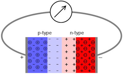
A sequence of metal contact, n-type semiconductor, p-type semiconductor, and metal contact yields a semiconductor diode, pictured left. At the interface between n- and p-conducting materials (p-n junction), the mobile charges (shown within circles in the figure) recombine, while the fixed charges (negative in p-conducting and positive in n-conducting material) remain. This produces a boundary layer that has a lower concentration of mobile charge carriers but still the usual concentration of fixed charge carriers and gives rise to a "potential wall" that hinders the subsequent flow to other mobile carriers and limits the thickness of the boundary layer to less than one micron.
A solar cell is so thin that the sunlight penetrates to the p-n junction. There, by the internal photoelectric effect, the light energy is converted into a mobile electron and a mobile hole. Some of the newly created electrons manage to move away from the boundary layer into the n-type region, and some of the holes succeed in moving into the p-type region.
Unfortunately, the majority of the charge carrier pairs created by the light energy recombine in the boundary layer, and this limits the efficiency of silicon solar cells to less than 25%. However, if the charge carriers do make it out of the boundary layer, the potential wall prevents their return. If the outside edges of the n- and p-conductor layers are connected by a wire, these carriers can combine only in a roundabout way through the electricity consumer, because the resistance of the wire and even a consumer is smaller than that of the boundary layer. A single solar cell generates about one volt. Inverters are used for the transformation into altering current and for generating greater voltages.
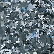
Thin-film CdTe modules are so-called II-VI-semiconductors, which are used in addition to III-V-semiconductors (GaAs) and the common tetravalent semiconductors like Si or Ge. The Roman numerals II, III, V and VI describe the valence of each component of the material. The Cd-Te combination can be cheaply manufactured on a large scale, but higher efficiencies can be reached with GaAs cells. Si materials can be divided into mono-crystalline (higher efficiency) and polycrystalline (better price/performance ratio). Pictured right is a polycrystalline wafer, about 10 cm in size. The so-called "thick layer" Si wafers are about 250 µm thick, whereas thin-film cells have a thickness on the order of 10 µm. They are produced from crystalline material with high efficiencies or from cheaper, amorphous material. Even cheaper and easier to produce solar cells are expected in the future from organic semiconductors. So far, however, polymers have only achieved low efficiency and durability. There are no expected shortages of material for polymers and silicon, but it could be difficult in the future to find sufficient resources of indium, gallium, tellurium, and selenium. Solar cell innovations and details can be found at Wikipedia.
Solar Star is a 747-megawatt photovoltaic power station in California. It consists of 1.7 million solar panels spread over 13 square kilometers, and had the world's largest photovoltaic capacity, when completed in June 2015. At the end of 2024, Solar Star is number 40 in the list of the world's largest photovoltaic power plants.The leading positions have moved to Asian countries. China is now the number one in the world in the growth of photovoltaics and as photovoltaic power producer in terms of total installed capacity and even of growth per capita. As of the end of 2023, the United States achieved 238 gigawatts of installed photovoltaic capacity in solar farms as well as local distributed generation. Solar farms generated 3.9% of total U.S. electricity.
Several criteria are used to assess possible applications of the PV system. The assessment of the economic payback is complicated by the fact that no accurate predictions are possible, based on state subsidies of PV power generation and the development of electricity prices. A more easily calculated parameter is the energy payback time, which is the number of years required for the PV installation to generate the same amount of energy (in kilowatt hours) that was spent on its production. A thin-film module system can pay for itself in about 2−3 years. PV power production with polycrystalline cells need 3−5 years, and those with mono-crystalline cells require 4−6 years. This assumes optimal sunshine conditions. In Chicago, twice these times may be required. The balance becomes negative when the calculated payback times exceed the estimated lifespan of about 20 years.